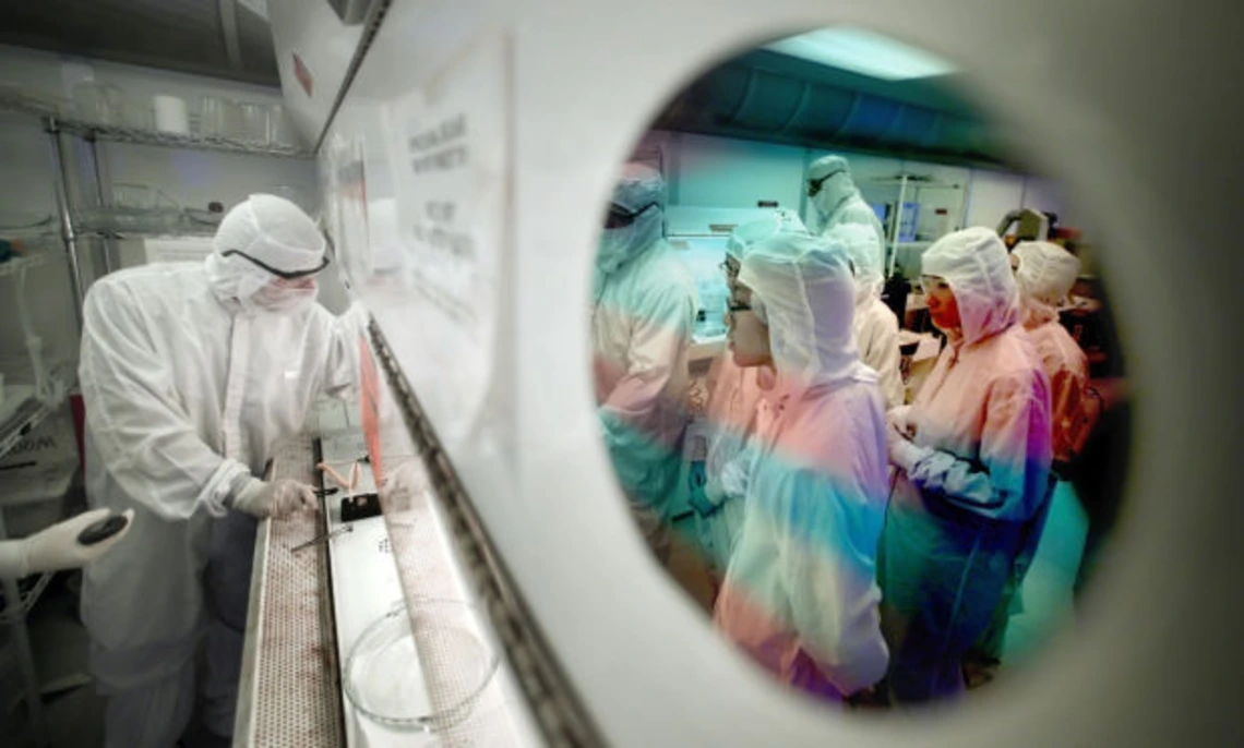
MSE Clean-Room Lab Helps Students Prepare for Spotless High-Tech Jobs

A revitalized clean-room practices lab at the University of Arizona aims to make its students more marketable for high-tech jobs after graduation.
The two-credit course, titled “semiconductor processing lab,” is part of the engineering program in the Department of Materials Science and Engineering.
This is the newest semiconductor processing lab at the UA and is open to both graduate and undergraduate students, says department head Pierre Deymier.
The class educates students on tool sets and processes required for the fabrication of structures that may be used in integrated circuits, memory devices, biomedical sensors and more.
For undergraduates who have taken the lab, there are better internship opportunities available, especially in the Phoenix area.
“There’s a lot of opportunities,” said Professor Srini Raghavan, who teaches the lab course. “Chandler and Queen Creek is Intel country. We are really in the heart of semiconductor manufacturing.”
“My students get these jobs after graduation,” he said.
Diane Haiber, a materials sciences and engineering undergraduate junior, got an internship this summer after marketing her skills she learned from this semester’s clean-room lab.
“This lab provided me with the hands-on experience and lab skills,” she said. “It helped me stand out better, for sure.”
The facility is the only class-10 certified clean- room facility on campus. For a lab to be certified as a class 10 facility, things must be carried out and operated in a clean environment with no more than 10 particles sized at half a micron or larger per cubic foot of air.
In perspective, one particle of sand is sized at about 100 to 10,000 microns.
The best clean-room standard is a class 1, which companies like IBM and Samsung use. Then there is the class 10 standard up to a class 100,000 standard.
Many challenges come with keeping a clean-room facility open.
First, high-tech companies are about two generations ahead of universities in their technologies, which makes the equipment available for the classroom rather archaic, according to Raghavan.
Second, it takes a lot of money to operate a class 10 lab, Raghavan said. For example, the lab’s fan must constantly circulate the air, which can be costly.
The UA’s interim vice president for research, Jennifer Barton, contributed about $2,500 toward the clean room’s funding. Additional funds came from differential tuition from the department, a joint program between Intel and the College of Engineering, and an extra student fee.
The lab has a 15-student capacity. Most of the lab’s students are from the College of Engineering, but Raghavan said he is able to relax the standards for anyone interested in the course who has taken some science and engineering classes. He recommends taking his preceding course, “semiconductor processing,” first.
Before taking the lab, students must complete an online safety course that takes no more than a couple of hours, and pay a $100 fee that is added into tuition.
“A hundred dollars is nothing when you consider the payoff of experience and internships,” Haiber said. “In the end, it pays for itself.”
Students enrolled in the lab will work with Raghavan, facility manager Omid Mahdavi, and two other staff members, Gregg Cure and Steve Orozco, who explain how the lab’s tools work, how to handle hazardous chemicals and more.
Currently, students are working on handling and cleaning silicon wafers or round disks that cannot come into contact with oils, particles or any metals. Eventually, the students will learn how to etch patterns on the disks and format layers.
While students write their reports individually, they work as a group, which Raghavan said is important for them to learn before entering a workforce.
“It’s critical that our students not only understand science, but can also operate in future workforces,” Deymier said. “It’s the key element of our curriculum — to get them jobs, good jobs.”
See the full article here.
Photo courtesy Arizona Daily Star
