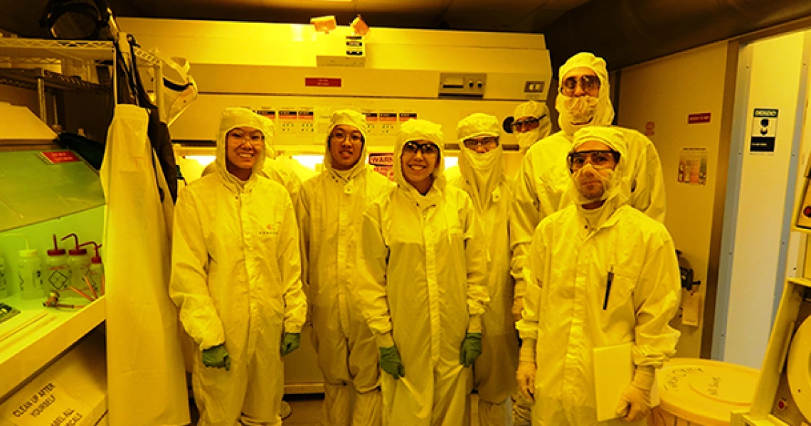
MSE Lab Trains UA Students in Cleanroom Practices

A new lab class in the “cleanest” environment on campus is helping prepare UA engineering and science students for high-tech jobs.
Cleanroom facilities at technology manufacturing companies are critical for designing and producing integrated circuits, memory devices, biomedical test structures, and the like. So there is a growing need for employees trained in cleanroom practices.
The two-credit elective, Semiconductor Processing Lab (MSE 447L/547L), is made possible through funds from the Intel-UA College of Engineering program in materials science and engineering. The lab opens up opportunities for internships and jobs in industries that value cleanroom manufacturing, and it makes graduate students more aware of research facilities and equipment.
“Many employers are impressed when they hear that a student has gone through formal training in fabricating structures in a cleanroom,” said materials science and engineering professor Srini Raghavan, who teaches the lab. “Students have an increased edge over their peers during the hiring process when they are properly trained in these types of procedures.”
The class is offered in the spring to students in all engineering majors and is preceded by a preparatory recitation (MSE\ECE 446\546) in the fall. Students in the lab learn how to gown up to work in cleanrooms and proper handling procedures for chemicals and materials inside a cleanroom, and they become familiar with various fabrication tools for micro and nano structures.
Engineering undergraduate student Diane Haiber said she now attends career fairs with an added level of confidence, thanks to the class.
“The course is structured so that students get hands-on experience through implementation of various fabrication and processing techniques: so far we have done wafer cleaning, thermal oxidation and photolithography,” she said. “And learning goes beyond the lab activities; Dr. Raghavan shares his own experiences from when he worked at Intel.”
Added graduate student Jivaan Kishore, “Not many universities offer such a comprehensive training program with respect to semiconductor processing.”
The class uses the only Class 10 certified cleanroom facility on campus, the Micro/Nano Fabrication Center, or MFC, housed in electrical and computer engineering.
The center’s manager, Omid Mahdavi, said the facility is a prime example of university-industry partnerships, one of the overarching themes in UA President Ann Weaver Hart’s recently unveiled “Never Settle” strategic plan.
“Most of the operational costs of running the MFC facility are covered by space and services offered to industrial clients who have on many occasions hired UA students,” said Mahdavi. “Here we have a lot synergy between academic and industrial activities. In a sense, President Hart’s Never Settle strategic plan has already been in motion here at the MFC for a number of years.”
The Micro/Nano Fabrication Center Lab in the ECE building is mostly a Class 100 facility and offers a limited Class 10 work environment. To put that classification in perspective, large semiconductor companies, such as Intel and Samsung, manufacture their products in Class 1 cleanrooms where there is no more than one particle the size of half a micron for every cubic foot of air. In contrast, the outside air generally contains more than 30 million particles of dust per cubic foot, which would equate to a Class 1,000,000 rating, also called room air.
The UA is home to two other cleanrooms: a Class 1,000 environment maintained by the chemistry department, and a Class 1,000 to 5,000 environment maintained by the College of Optical Sciences.
See the full article here.
